
Two-dimensional gratings are ideal for positioning and metrology applications that require exceptional accuracy (~ nanometers or less) over a long range (~ millimeters or more). These requirements are found in the semiconductor, precision manufacturing, and biological imaging fields, to name a few. Often displacement measuring interferometers (DMIs) could provide a solution, but might also pose expensive or even impractical system constraints. A grating-based interferometer offers a simpler, more robust solution.
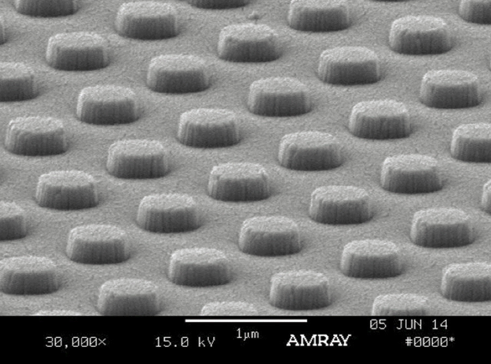
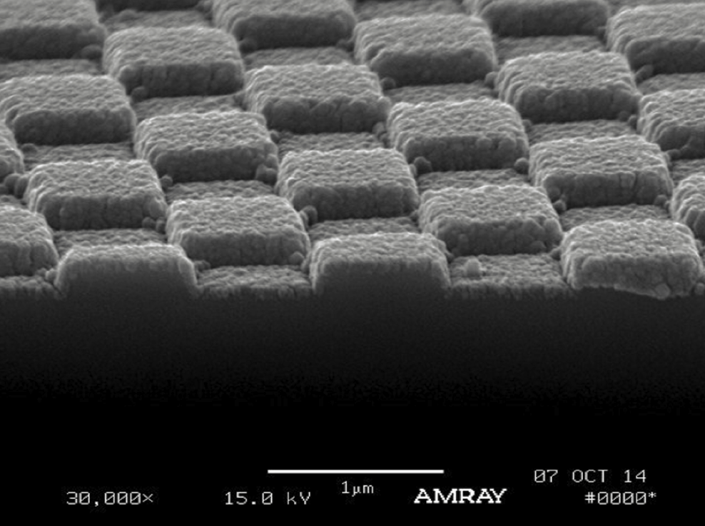
2D gratings are produced by orthogonally overlaying two one-dimensional (1D) structures. The result is a rectangular array of grating features for which the net diffraction efficiency is equal to the product of the two 1D efficiencies. With exceptional control over the placement accuracy of grating features, PGL’s 2D gratings provide an industry-leading solution for the most demanding positioning applications.
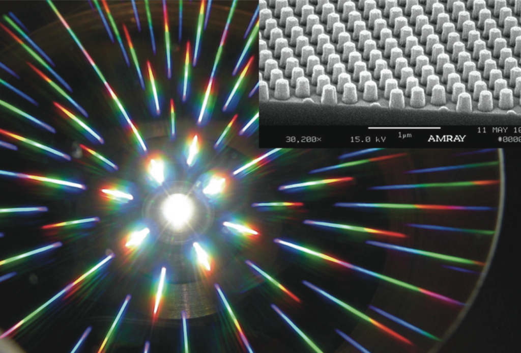
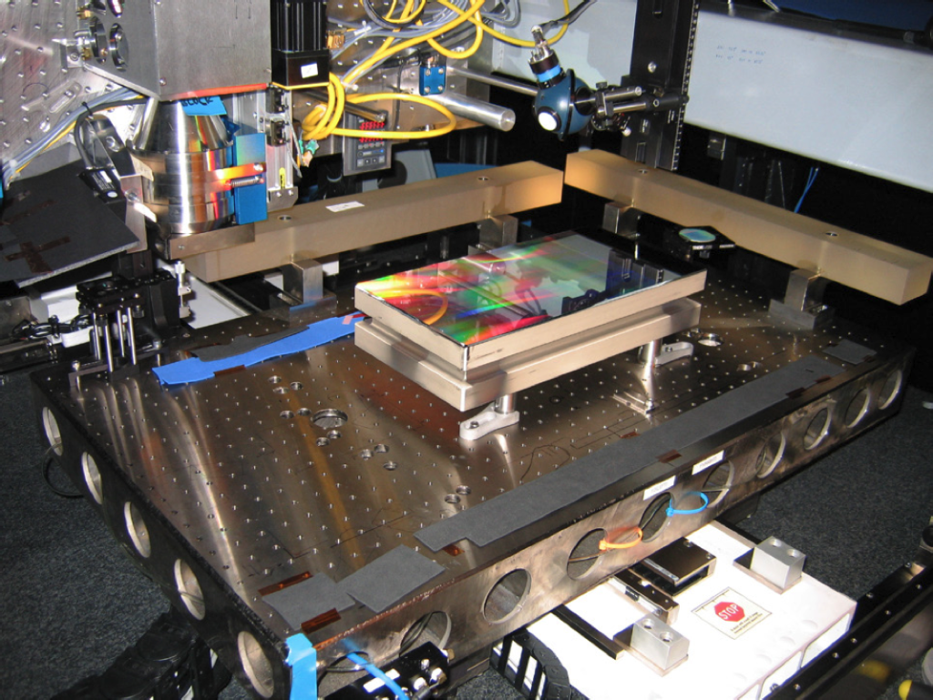
The high accuracy of PGL 2D gratings starts with the Nanoruler, based on the proprietary SBIL (Scanning Beam Interference Lithography) technology developed at MIT. The Nanoruler comprises a precision air-bearing XY stage with dual-axis DMIs mounted on an active vibration isolation system and housed in an environmental enclosure which controls temperature to ± 0.01°C. It scans a small beam of fringes that are actively stabilized with heterodyne phase reference interferometry across a large substrate in any direction, and with real-time variation of the fringe frequency and orientation.
Averaging methods and excellent dose control ensure consistent period and feature shape across the grating and from part-to-part – period repeatability has been shown to exceed 10 ppb! Systematic defects found in holographic grating writing systems are all but eliminated. SBIL even allows programmable correction for wavefront errors in substrates and other system-level imperfections.
These features, combined with a lack of fundamental limitation on substrate size, mean PGL’s SBIL process is the ideal solution for large, 2D gratings.
5 Commerce Way, Carver, MA 02330, USA|+1.508.503.1719|sales@plymouthgrating.com