Reactive Ion Etching

Reactive Ion Beam Etching (RIBE)

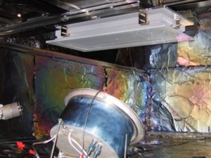
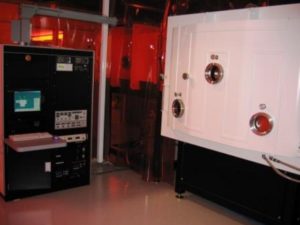
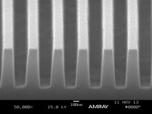
To transfer a photoresist grating pattern into the glass substrate, PGL utilizes a custom reactive ion beam etcher specifically designed for fine dimension control and pattern uniformity on large substrates. Up to meter-sized substrates are mounted grating side down at the top of the chamber. Etching is performed by reactive gases and a gridded radio-frequency (RF) ion source. A unique x-y scanning stage maximizes uniformity by moving the substrate through the beam during the etching process.

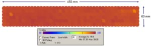
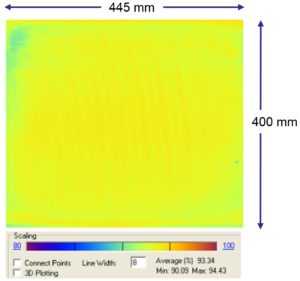
PGL has also developed a custom optical monitoring system that allows in-situ measurement of grating diffraction efficiency. Because this system utilizes the scanning x-y substrate stage, it enables not only the optimal efficiency, but also excellent uniformity especially for metal-coated gratings.

.
PGL’s custom, large-format RIBE system with scanning x-y stage.
Reactive ion beam in action.
Diffraction efficiency map showing a highly uniform 460 mm x 70 mm MLD grating on fused silica etched with PGL’s RIBE system. The average DE is 98.9%, with a minimum of 97.4% and a maximum of 99.3%.

Plasma Reactive Ion Etching (RIE)

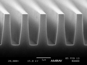
PGL has also developed an RIE process in its RF plasma reactors for very deep etching in fused silica. This process is particularly important for transmission gratings, as these require deeper grating grooves. It is capable of producing exceptionally smooth, deep, high-aspect-ratio grating grooves. Groove depths as deep as 2.5 µm are routinely produced.

SEM of 2.5 µm deep, 800 lines/mm grating produced with PGL’s RIE system.
SEM of 0.65 µm deep, 2,400 lines/mm grating produced with PGL’s RIE system.
Diffraction efficiency map showing a highly uniform 470 mm x 420 mm fused silica transmission grating etched with PGL’s RIE system. The average DE is 95.7%, with a minimum of 92.4% and a maximum of 96.8%.
Plymouth Grating Laboratory is dedicated to making the highest-quality diffraction gratings available today. Our focus is on lasers and laser systems. PGL gratings offer exceptionally high diffraction efficiency and laser damage threshold, combined with superior wavefront error and uniformity over large areas. This performance is made possible by PGL’s exclusive use of the Nanoruler, based on the proprietary Scanning Beam Interference Lithography technology developed at MIT, and PGL’s industry-leading process expertise. The company occupies 20,000 sq. ft. of dedicated manufacturing, engineering, and office space in Carver, MA, just outside of Plymouth, and about 45 miles south of Boston.

5 Commerce Way, Carver, MA 02330, USA|+1.508.503.1719|sales@plymouthgrating.com

© 2024 Plymouth Grating Laboratory|All rights reserved|Design by CleanClearCreative.com